
The image to the left is a Motorola CableCard. Doesn’t that sentence sound familiar? I’ve written previously about the subject.
Click on the image for a much higher 9875 x 16046 detailed view.
I’m still scratching my head and trying to find a perfect solution for digitally scanning any arbitrary PCB, regardless of placement or onboard components. The fact is, I haven’t yet found a good all-round solution.
The CableCard PCB here was scanned using a flatbed scanner at 6" x 6" at 4800dpi. Each side took 4 minutes to scan. The resulting images were 19200 x 19200 at 1.1GB each. Larger than I’d first thought, although disk and memory is cheap. The more pixel detail I get - the happier I am.
As with any project, the top and bottom layers had to be brought into Photoshop and manually aligned and inverted using the same technique I’ve written about before. This allows me to quickly flip the board over virtually in-order to follow PCB traces without distracting my eyes.
If you’re interested in the pinouts for the device, and the protocol, you should checkout this slightly older CableLabs CableCARD Interface 2.0 Specification document. The newer versions of this document don’t bring much to the discussion, they’re not worth chasing down for this article.

Here’s the same quality scan of the bottom layer. Not a lot going on here.
Before I go any further I need to point out a few things. I purchased this Motorola MediaCipher card from eBay a few years ago, along with a few others. Over the years I’ve collected a series of CableCard and I’ll probably open up another brand for comparison in the future. I haven’t rented it and I have no idea when the card was last used.
My goal isn’t to circumvent security or knowingly violate any laws.
Ass covering said… You should reaslize that CableCards are going cheap on eBay, $10 or so.
In terms of receiving TV signals they’re useless to me as my MSO (Cablevision / Optimum) uses Cisco/NDS based cards. That being said, they’re still useful for doing teardowns and testing interaction with CableCard receivers, when no RF connected or when monitoring the message control bus.
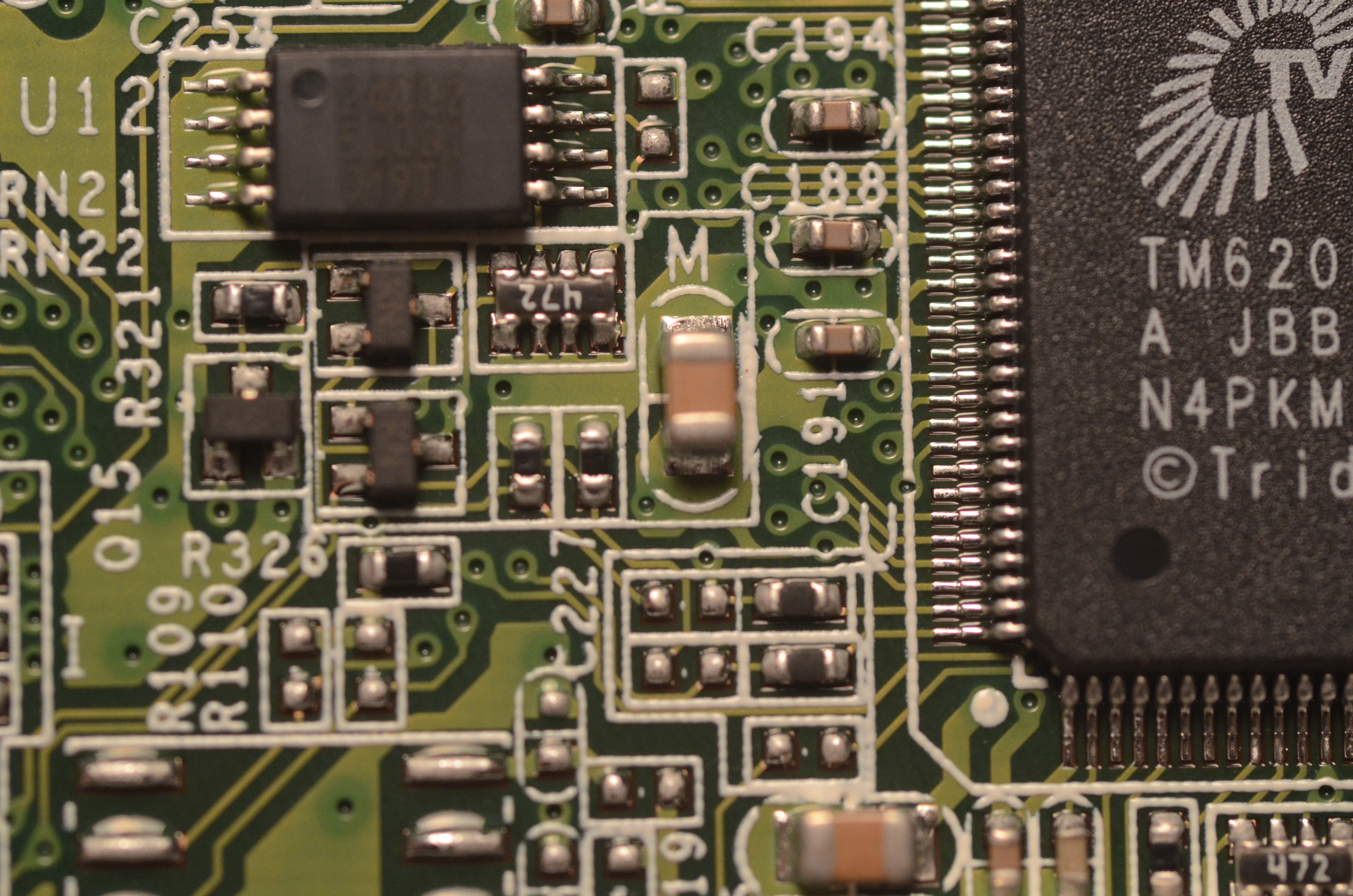
A couple of immediate observersations from both PCB layers
- SCF6100VM - Freescale Microprocessor, image
- 320W18BD - Intel Fash Memory, family datasheet, image
- D9GRQ - Micron SDRAM, family datasheet, image
- Battery. image
All the major PCB traces are buried between layers running to and from the BGA packages, to be expected and infact required for CableLabs device certification. I didn’t expect to find a completely exposed bus to the flash or SDRAM.
Sidenote: The CableLabs cert requirement specifically says (paraphrase):
The device should be tamper resistent and thus prevent access to restricted keying material. […] prevent access from any person using readily available and inexpensive debugging equipment.
A battery! - Perhaps keeping the SDRAM alive while the device is not connected to a host?

I continue to find small but annoying issues while using a scanner on PCBs.
Have you noticed the shadow next to the package on this image to the left. I’m reasonably sure I could clean that up in Photoshop - still - its a hassle. I also find that most PCBs don’t sit flat on the scanner glass, which causes some minor off-angle scanning issues including the inability to perfectly align. I get close, close enough, but I’d like to align a little tighter than what my scanner allows. This fluctuation tends to skew the pcb traces by a millimeter between layers.
All things considered, the effort it took to scan and manually align both layers was probably 30 minutes, still trivial by any measure.
I started adding layers in Photoshop for comments as well as sketching out the major control interfaces looking for any obvious interconnects. I didn’t find much of interest but I will point out two or three interesting things.

Firstly this, the cablecard has pins 6, 7, 8 connected from the 68-pin header directly to the SOC.
These pins are unused in the specification and would not expect to be driven by any ‘in spec’ CableCard device. Either designers want to screw with anyone looking at the PCB, or more likely, its some kind of manufacturing or diagnostic interface which needs a custom test device to interact with it.

Looking at the PCB, the ground plane doesn’t flood the entire PCB. Its possible to see buried traces in some parts of the design using a bright light source.
This image is much poorer than I’d like but it demonstartes a useful technique.
I used a flashlight on the underside of the PCB then took the image using an iPhone looking through the eye-piece of my optical microscope. You can clearly see the edge of the battery and a few traces. Some of those traces are actually visible on the bottom of the PCB (not buried), but when I repeat the same test on other parts of the PCB I can clearly see a few buried traces.
I should pop a camera into the Microscope, a future project.
The overall effect is much more interesting when you’re just examining the ground plane edges directly through the microscope, and no iPhone is involved.

Here’s the cablecard message/control bus, where the host device sends messages to/from the CableCard to request service information, query conditional access states, select tv channels for processing, as defined in the CCIF 2.0 document mentioned earlier. Its a lot like a SPI bus in terms of its electrical activity, along with a couple of adjustments as covered by the CCIF 2.0 spec above.
During debugging I inserted the card into a working HDHomeRun and looked at the control lines using an oscilloscopee. The Host is communicating with the card, its responding and alive, communicating at a rate of 6.75MHz. It would be trivial to tap some debug wiring onto the resisters and hook all four signals into a logic analyzer for inspection. The control bus is a very close relative to SPI, easy to inspect.
Warning: Even if you wanted to, trying to modify the messages to/from the host and CableCard would not breach any security. Any important messages are securely signed between the host and CableCard to prevent man-in-the-middle tampering. That being said, reading the bus can be useful when debugging behavioural problems.
On other pins I see the 27MHz transport in/out clocksi, a pair of 8bit parallel TS data buses - so everything appears to be alive in the card.
The test pads are all active. I only measure clocks and gpios or various voltages. I don’t see any control messages, although I didn’t try measuring when exercising the flash or booting the device). Given enough time and patience, all the test pads should be monitored during a series of power up, boot and reset exercises.

Sidenote: I once built a small project based around a Cypress FX2 Microcontroller and a PCMCIA extension board in-order to intercept and record cablecard control messages between the host and CableCard directly to a PC. I plan to write about this in a future article, but in the meantime here’s a quick teaser.
The cablecard inserts into the PCM extender / adapter upside down, the FX2 microcontroller monitoring (read only) the communication between card and host.
The PCB has two rows of 13 test points. Similar to the other named test points, I saw nothing other than clocks, voltages and possible GPIOs on these. But, like the test pads mentioned previously, I didn’t try measuring when exercising the flash or booting the device).
Given enough time and patience, a lot had be learned about this physical cablecard design simply by repeatidly power cycling the device while monitoring the various test points.
If I was trying to obtain the contents of the flash I’d probably remove the solder mask on the VIAs in and around the flash (grind it off) and look for activity during boot. Or, Hot air the flash BGA, remove it off the PCB and insert it into a reader.
or… ask someone on a Comcast, TWC or FIOS plant to run a Linux app for me, so I can gather the firmware directly from their plant. Some of the MSOs broadcast set-top-box and CableCard firmware using regular QAM channels, while others use the OOB. This is an easy and first approach I’d take - if I wanted their firmware.
Questions
I’m not too sure what the Freescale CPU is. I’ve googled a little and it looks like a custom CPU by Freescale for Motorola, so its probably based around an existing (well document) cpu that Freescale were selling during 2002-2002. I see lots of Freescale documentation on the web for their Secure ColdFire (SCF?) technologies.
Its a curious CPU for sure.
Write to me if you know anything about this chip, details on the contact page.

The image to the left is a Motorola CableCard. Its thicker and about the size of a credit card.
CableCard is a United States CableTV content access and copy protection device. Similar devices exist in Europe. Its designed to translate the highly proprietary television signals being transmitted by your Cable Company (MSO), into one agreed national standard. That’s a good thing. It creates one electrical interface and a fixed set of control protocols. Companies other than your MSO can therefore develop new consumer devices that interoperate with CableCard, offering consumers more choice and higher flexibility.
Why should we care (background)?
For the last 15 years, the general consensus in the United States was that MSOs rented set-top-boxes to consumers, who rarely if ever had any kind of choice. The quality and usability of these boxes was poor at best and offered nothing in the way of choice or features. The MSOs (by the opinions of many) were not doing enough, little or no innovation was taking place while consumer cable bills were gradually getting higher and higher. The vast majority of technically minded people thought the MSOs did ‘just enough to get by’. To make matters worse, due to the geographic size of the US as well as the cost related to rolling coax to homes, rarely if ever did a home have access to more than one cabletv network. The local MSO had a monopoly.
The Federal Communications Commission (FCC) took action. They mandated that the cable industry should offer choice to consumers and open up access to their proprietary cable networks. This is why companies such as Tivo can build third party set-top-boxes that include all sorts of interesting features including video streaming, internal transcoders that convert TV to iPad and mobile phone formats, as well as providing better user interfaces, in-home streaming, scheduling recordings from your phone and more responsive on screen TV guides.
If you live in the US and are thankful for Roku, Amazon, Google set-top-boxes that now offer Netflix, Amazon Instant Video, HBO2GO, YouTube and generally more attractive user interfaces, the seeds of those boxes were born out of companies like Tivo, who saw this new technology as a way to provide better experiences in the home (based around TV), and saw the up-take of CableCard by consumers as a sign that disgruntled subscribers wanted better video experiences.
I’ve worked as an engineer on a number of commercial CableCard projects, I’ve read the specs, I’m privy to all the secrets, worked in detail with the hardware. I know the benefits and the warts. CableCard is not a perfect technical solution but its a good start.
We should all care
… which brings me to the point, it’s such a pity its going away.
Everything I’ve read on the internet suggests that Comcast are a) morally bankrupt b) happy to squeeze the American public dry and c) not too interested in keeping their customers happy.
That being said, credit where credit is due. They’re launching this new feature for people with visual difficulties, I like it. Well done Comcast!

I decided to spend saturday morning digging into the Elgato Game Capture HD 60FPS encoder, partly because I felt like taking a deeper look at its design and partly because my prior imaging article was a trip down memory lane. I thought I’d try a different imaging technique then dive into the hardware for a few minutes.
The board itself is pretty flat, no high-rise capacitors, no protruding headers so a quick scan of the board in the Cannon 8800F scanner produced a couple of useful 600dpi TIFF images without too much trouble. I later converted to PNG, the full resolution images are here. See board top and board bottom.
While its tempting to dive in and start looking at the components, that would be a distraction. The primary goal for today was trying something different in Photoshop. I wanted to import the PCB images and align them correctly on different layers.
If they’re positioned correctly in relation to each other then I’d be able to rapidly switch between layers and follow traces faster than physically handling a board. IE, performing a virtual board flip, backwards and forwards with the click of a mouse, all while keeping my eyes focused on a specific VIA. This trick, should it work, would enable faster debugging of a PCB when I don’t have access to schematics.
Another good reason for adding new layers, I wanted to add additional comments, coloring and routing information and have that detail be stored inline with the PCB images, not on paper. Paper records can easily be lost.
Fair warning: If I talk about the components on the PCB or discuss them at all then consider it a bonus.
Step 1 - Flip the bottom PCB image so that all layers are viewed from above
Load your top and bottom PCB images into a new Photoshop image:
Menu, File / Scripts, Load Files into Stack.
Here are the two PCB layers in Photoshop, I’m flipping between the two visible layers, notice the problem?
When I scanned the original PCB, I scanned the top layer first, flipped the board over, being careful to keep the connectors in the same place, then scanned the bottom layer. As a result, the visual view is from above and below. I need all the layers in Photoshop to be from above, so when flipping through the layers I’m looking through the board from the top, not inverting the view as if looking from beneath.
Its a simple fix, Select the layer you want to flip, then Menu / Edit / Transform / Vertical, now toggle through both layers in Photoshop and you should have a top down view of both PCB surfaces.
Step 2 - Properly aligning the layers

You’ll notice the PCB layers don’t quite line up in the video above. I selected the bottom layer and performed a series of minor rotations and canvas moves so that some key PCB components and markings were stacked perfectly above each other when flipping layer views.
To do this, select the bottom PCB layer (which is the top most layer in the Photoshop stack) and adjust the opacity to roughly 50%. This allows us to view both images concurrently. See this higher resolution screenshot for finer detail.
Use the Photoshop Move tool and the control key for finer movement control. Place the PCBs exactly over each other. Once done, you should be able to adjust the opacity of the bottom layer from 0 to 100% and assuming you’re rotation and alignment is good, the PCB layers should now be properly placed.
For demonstration purposes I’ve created a new top most layer, highlighted in red a couple of things you should focus your attension on, then adjusted the opacity to highlight the effect. I took a short video to demonstrate the final alignment.

Its also worth taking a moment to cleanup the image a little more. I used the Magic Wand selection tool and highlighted the PCB, inverted the selection mask (to select everything else outside the PCB) and deleted all of the unwanted pixels. Here’s an updated image.
A quick .5 degree rotate clockwise brought the image slightly more vertical.
With close inspection the images aren’t perfectly aligned, the top image is 2% smaller than the bottom image, which leads to small issues on the right hand side of the overall project. That being said its definitly close enough for my goals.
Step 3 - Pull the datasheets and create layers with additional comments

For each major component on the PCB, add any additional notes to the layer using Text and line drawing tools. The benefit of this is that as you explore the board and mark up any traces, pins or VIAs without trashing the original PCB pixels, and you can enable/disable the debug layers easily as you later need to add or remove additional visual detail.
Check the datasheets and mark up any relevant pins or points of interest. I tend to start with I2C and board wide Resets. If no datasheets are available and Google doesn’t help then its a manual exercise requiring you to probe the pins with a meter to check for continuity or look at the pins with a scope while the device is active to spot any obvious buses.

I noticed that when zooming in that the image resolution quickly starts to deteriorate. Most likely, higher resolution PCB scans are required for serious use. Either I need a better scanner or I should spend the time to use the digital SLR.
At this point in time my general goal is complete, it was pretty trivial to import PCB images, align them and add additional notes and layers. Here’s a sample image.

… and the higher resolution version.
Technical Follow-up
Interesting, a 32bit Micro and SPI flash!
I had a hunch that the NUVOTON NUC100 keeps track of the HDMI input and output format negotiation process, for when the software isn’t running so that video passthrough works reliably.
I dug into the I2C traces to look for that. Additionally, I suspect it loads its firmware from the SPANSION flash, positioned fairly close to it, and this uses a SPI bus.
I dug into the SPI traces but was unable to prove the SPI was used by the microcontroller. Most likely its used by the Fujitsu video encoder.
At this point the Reset lines have been traced and I2C.
The NUVOTON has the following I2C connects:
I2C Bus 1
- Direct to the DibCom 0700 USB controller.
I2C BUS 0
- CAT6612 HDMI TX
- P15C Power DC Related
- Cirrus 42L51C Audio Codec (ADC)
- MStar MST3367 HDMI RX / SOC
Time for some I2C debug fun
I took a couple of quick I2C bus traces using a logic analyzer on the pins highlighted below:

No surprises, I2C traffic on the buses.


Photoshop, a swiss-army knife for pixels!
Questions
How do you generate a large-scale and fairly precise image of a PCB, so that you can look at it for hours without straining your eyes, where do you begin?
What happens when you take a series of high resolution images of a PCB while hand-holding a DSLR, then try to stitch them together with Photoshop?
Background
A hardware schematic is a ‘road map’, that shows how all of the components on a PCB are connected.
I occasionally work on projects to create new Linux drivers for hardware that is relatively closed and proprietary, where we don’t have access to hardware schematics.
Having the schematic is ideal but more often than not, the manufacturer is unwilling to provide schematics, datasheets or other support materials without signing highly restrictive Non-Disclosure Agreements.
Developers need a good understanding of the hardware to be able to create useful drivers. The project becomes much more difficult without a schematic and an understanding of how the hardware components are wired together. Occasionally I make a PCB image for a commercial project, other times I’m simply curious so I poke around some random piece of hardware to understand it, to see what we can learn.
In early 2011 I took on a project to create a Linux driver for the AverMedia H727 HD capture card. The project was for a UK customer, it was not funded in any way by the hardware manufacturer. The card itself is now sold in a couple of variations, with and without a DVB-T digital TV tuner/demodulator. Both versions support raw video capture from standard definition 720x480/576 up to 1920x1080i on HDMI and Component inputs, as well as traditional standard definition resolutions via svideo / composite. The card has some interesting capabilities.
To support the project I needed a schematic or something close to it.
This article describes how I generated an image of the PCB along with the tools and processes involved.
While I didn’t end up with a schematic, the final image did contain enough detailed hardware information that I found it invaluable.
Goals
-
Generate an image or floor plan of the PCB top layer, showing the interconnects between the PCIe Controller, the Component Video Decoder and the HDMI Video Receiver.
-
The image should contain enough detail so that I can zoom in to pin-level details. I expected to follow traces all over the board, print, snapshot and comment on routes, marking them up on paper with notes and comments. I’d later archive these paper records along with the other project notes.
-
Avoid using a magnification eyepiece in order to inspect the PCB. Over long periods of time they tend to strain your eyes. This would allow me to look at the PCB in great detail during extended debugging sessions.
The device had some other interesting components, some small analog-to-digital audio sampling devices. I needed to understand how all of these parts were wired, and ultimately how they were being controlled.
The Procedure
Here’s the procedure I used along with commentary from 2011 and 2015. I’ve left it in as you may find it interesting. I’ll close the article by highlighting any mistakes and pointing out any lessons learned.
Step 1: Take a sample picture and see how much detail you get from the camera
I happen to have a Nikon D7000 DSLR. I’d picked up a AF Micro Nikkor 60mm Macro lens from eBay a while before this, mainly for nature photography. I pulled out the camera, hand held it, no tripod or stabilization rig, placed the PCB on the bench and took a shot of a small part of it.
You don’t need an expensive camera but you do need a macro lens to get higher levels of detail.
Here’s an example macro photo, DSC_1803.jpg with a shallow depth of field, blurry cap tops but perfect PCB focus.

This is a 4928 x 3264 (16m pixel) shot of a small part of the PCB. I got to thinking, “what would happen if I took 80 or so similar shots and stitched them altogether?”
I loaded the image into photoshop and looked at the detail. Not Bad, an awkward shallow depth of field was noticable and my light wasn’t perfect. The picture was promising so I continued.
Step 2: Take a number of photos then capture each part of the PCB
I took another 7 shots of the PCB starting from the top right hand side and slowly moving the camera vertically down to the bottom right, imaging a strip of the PCB with a 30% overlap between images.
After I reached the end of the strip, I moved the camera left and back to the top of the PCB, imaging the next strip, making sure that I had roughly 30-40% of the strip to the right hand side inside the shots of this new strip. This over sampling of data would produce useful tracking and reference points when I expected to process the images in PhotoShop. I expected it would correctly align and join the images based on this oversampled pixel data.
All in all I scanned 10 strips, slowly digitizing the PCB from right to left, each with 7-8 images, roughly 80 JPG images for the top layer of the PCB. 6MB per image meant I’d collected approximately 480MB of files.
Did I really need this amount of detail? No, not really. It was a saturday morning, my wife and kids were out of the house so I had a free morning to learn, experiment and make a few mistakes. By this point I was curious to see how the mornings imaging project would turn out.
DSC_1824.jpg - Above image. This is the lower left hand side of the PCIe controller. Pin sharp and looking ok for a hand held image.

DSC_1820.jpg - Above image. Blurry - look at the pin sharp detail at the top right vs the bottom left, a sure sign that I have a very small depth of field. The distance between the top right of the PCB to the cameras focal point, vs the distance of the bottom left to the same focal point was different. I was hand holding the camera. Hmm. If this continued, how would this effect the Photoshop merge? I continued regardless.
Step 3: Image merging in Photoshop
Not every tool I use is free and open source. Life is about choices and also using the right tool for the right job, or simply working with a tool that you’re comfortable with. Photoshop is a world class product that I use for various projects. I’ve used Gimp in the past, I’m simply not interested in using it for these kinds of projects.
I used a 2.8GHz 10GB Ram MacPro, 8 cores which at the time was a lot of CPU and RAM, by todays standards its average.
I started by trying to merge all 80 images simultaneously into Photoshop (CS5). This was a big mistake. It ran for 30 minutes with little feedback, it appeared to have hung. Unhappy, I gave up hope and aborted the process.
I found the best method was to merge the 7 shots from each vertical strip in Photoshop one strip at a time, breaking down the scale of the task into smaller pieces.
Here’s the settings I used, basically the defaults:
From the Menu, select File / Automate / Photomerge, select each image associated with the strip.
I numbered the strips 0-9, where the right most strip is 0 and the leftmost is 9.

Strip #0 took 2 minutes for Photoshop to Merge and the resulting composite image had dimensions of 5886 × 12532.
I saved the merged strip as strip00.psd, it was 540MB on disk. So I’d turned roughly 8 pictures of 5-6MB each into a 540MB collage. Larger than I would have anticipated and I needed to do this 9 more times.
The data Photoshop required in order to digest and produce the final composited image was significantly larger than I’d assumed. I wasn’t sure how well this whole exercise was going to end.
At this point I was committed, regardless of the outcome, so I repeated the process for all 10 strips.
Merging each subsequent strip 1-9 took around 2 minutes. 20-30 minutes later I had 80 images merged into 10 strips, saved to disk with names strip00-09.psd. Each PSD file varied in size a between 450MB and 750MB.
Step 4: Merge the Strips of images together
Then:
- Merged strips 0+1+2+3 into strip21.psd (output file 1.27GB)
- Merged strips 4+5 into strip22.psd (output file 720MB)
- Merged strips 6+7 into strip23.psd (output file 780MB)
- Merged strips 8+9 into strip24.psd (output file 680MB)
Here’s a screenshot of strip22.psd.

After producing strips 21 to 24 I consolidated again.
with:
- Merged strips 21+22 into strip31.psd (output file 1.5GB)
- Merged strips 23+24 into strip32.psd (output file 1.16GB)
After this I started the final merge, bringing strips 31 and 32 together to produce the final image. I Merged strips 31+32 into strip40.psb (output file 2.48GB)
PSB is apparently Adobe’s “Large Document” Photoshop document file format.
I don’t have the exact merge timing information but I’d budget 90 minutes to complete a similar merge in the future.
I took the approach of a small ‘divide and conquer’ approach with Photoshop. It wasn’t able to merge all 80 images in one session, but by slicing the problem into smaller chunks, I got photoshop working reliably, I guess much of the overlapping pixel data was being discarded after use by Photoshop, so breaking the problem into smaller chunks helped with the overall size of the dataset and thus processing requirements.
I also suspect that with more accurate camera placement I could have reduced the oversampling of pixels down from 30-40% to 10%, reducing the overall image data and therefore expediting the overall process.
Step 5: Load the final image and review
It took 38 seconds for Photoshop to load and display the final image. That’s a long time and it’s certainly the largest image I’ve ever needed to process.

Here’s a screenshot of the final image inside Photoshop. It was taken using the latest version of Photoshop (CC 2014) during Feb 2015. It took 25 seconds to load, a considerable improvement, thank you Adobe Engineering.
If you’re curious, the final image had pixel dimensions of 30448 x 16251, otherwise known as 494M/pixels. The PSB file on disk was 2.5GB.
Here’s a movie showing some basic zooming and navigation around the final Photoshop image. Not bad. Clearly some room for improvement but a great first attempt at this process.
Lets put this into perspective, a microscope could have easily improved on the resolution but by goal was to show these images on a large monitor over a period of weeks. While this project took and entire morning, the alternative was to stare at a PCB under a microscope for weeks at a time - not good for my eyes and impractical in terms of switching between the desk and bench.
How did the final image influence my work?
As the driver project progressed I referred to the PCB imagery literally hourly.
In terms of understanding the hardware, I used a mixture of debugging devices, such as affordable logic analyzers, a multi-meter and an oscilloscope. I was quickly able to deduce all of the important pins and routing information on the PCB. I could easily follow the traces between the front and rear of the board following the VIAs.
In practise, I’d zoom into small parts of the PCB and print specific areas for my paper notes. I’d scrible down thoughts and ultimately created a collection of notes about various aspects of the signalling and design. I’d find the datasheets for the analog audio encoder, look for the I2S digital audio signals and follow those through the traces into the PCIe controller. Once you’ve done this for all of the major audio, video and control buses, you start to get close to re-inventing that missing schematic.
Given the significant lack of components on the rear side of the PCB I had no need to image that side, everything I needed was generally available on the top. I did have to follow a couple of I2C traces via VIAs to the bottom and back, but that was simple enough using a traditional eyepiece.
The bottom side of the PCB was generally used for power routing, I had no immediate need to document or understand those.
Closing thoughts and Lessions Learned

My first mistake, see image above. I wish I’d taken greater care with the cameras depth of field and used a fixed camera rig to position the camera and the PCB at a fixed distance, keeping everything in focus and perfectly aligned. I held the camera by hand, which introduced too much vibration and motion. A minor mistake that lead to slightly blurry imagery, or parts of the imagery blurred.
For my next PCB scan project I’ll probably build a small rig on wheels so I can maintain a fixed focal length and aperture (to keep the images pin sharp). I’ll keep the camera on the rig and leave the PCB perfectly lit and completely parallel to the focal plane.
$30 on wood, screws and a cheap set of rollars should be enough to construct something.

My second mistake, see image above. While I said I tried to keep a 30% image overlap while photographing the board. Clearly I made a mistake and ended up with a small amount of missing (although ultimately) non-critical pixel data. This was once again the result of hand-holding the camera and not enough of an overlap between slices 0 and 1.
I don’t want to repeat this mistake in the future, as the missing pixels may be more problematic.
My next PCB scan will almost certainly use a homemade jig to help contain this kind of issue.
Note to self: I wish I could find a PCB house that would xray the board and give me a visual image of any PCB in the New York area.
It may also be possible to produce a better final merge by experimenting with Photoshops ‘Collage’ or ‘Reposition’ Photomerge modes, instead of assuming ‘Auto’ was good enough. Certainly some room for further experimentation. [Update: Its also possible that since CS5 Adobe has improved their merging technology further.]
Have you ever taken on a project like this? If so I’d love to hear from you.
I’ve written briefly in the past about the Saleae 8 Logic Analyzer. The Saleae comes with some traditional grabbers that connect your logic analyzer to the pins and wires of whatever it is you’re working on.
The grabbers work fairly well with chips that have a 1mm pin pitch. They also work well if you spend the time to solder debug/trace wires to your PCB. However, they’re useless when dealing with pin pitches smaller than 1mm which is all too common these days. In short, the grabbers are great for eeproms but completely impractical for use with tuners, demodulators and USB or PCIe bridge devices.
Note to self: I should probably source some finer pitch grabbers.

When I’m working on something and I don’t want to break out the soldering iron in order to tack down trace or debug wiring, here’s a trick I occasionally use. Its handy when dealing with .5mm and .25mm IC’s. Woah, hold on, I can’t see a thing in your picture - I hear you say.

Here’s a better shot. I’ve attached a pin to each grabber and I’m using the tip of each pin, which is roughly .4mm to touch the pins on the IC that I’m interested in probing.
The technique is awkward, risky and error prone but frequently a time-saver and the only practical option. I generally only use it for doing quick I2C bus captures, where I can repeat the process multiple times until I get a clean capture. You’ll need three hands, two to hold the probes, a third to hit the record button in the logic analyzer software.
Note to self: Build a custom application that samples the microphone audio input, here’s me shout “NOW” across the room then automatically starts or stops the software.
If you try this pin technique then expect to spend 15 minutes doing multiple attempts, but its handy and useful if you can’t solder debug wires into fine pitch pins, or just need a quick and simple verification on some bus logic.
Fair warning: This technique adds unwanted capacitance to the bus that I’m debugging. Hence, I only use it with slower speed signals (less than 2MHz).
Use this technique with caution as you may accidentally short two neighboring pins and damage your IC.

Does this picture look familiar? Perhaps you too have a cramped PC chassis? My graphics card is to the left and the metal base of the chassis is to the right. In total I have 8cm (3") of room. Not enough to do any serious hardware work.
My problem is, I often want to debug a PCIe card that’s in that spare slot between the three blue PCI connectors. I don’t have enough room in this chassis to fit everything. The card, my hand as well as one or more probes all need space. What I really want is unfettered access to all the card components, without compromise, while the card is running under Windows or Linux in normal operation. I can’t be effective unless I can inspect card behavior ‘in-flight’. Look at the PCB image here, wouldn’t it be neat if I had that level of access to the board, with decent lighting around it, so you can attach to whatever components you want?

I’d be able to sit comfortably, attach multiple probes, easily see small components from any angle, my job of debugging and diagnosing the hardware would be greatly simplified.
A few years ago I discovered PCIe Extension Cables. PCIe is electrically a serial bus, which means it tolerates a certain amount of physical ‘extension’ to its lanes, unlike traditional PCIe which is a parallel bus and is much more difficult to extend. This PCIe extension capability is useful as it means the PCIe no longer needs to be on the actual motherboard.
Extension cables are cheap. Check Amazon for more details, you should expect to pay $7 or so. On eBay they’re $5 or so.


My cable is 18cm (7") long. On one end of the cable are the PCIe fingers that insert into your motherboard, at the other end is a replica of the PCIe slot on your motherboard. This cable extends the motherboard PCIe slot vertically and creates enough working room either side of the new connector to be useful. This particular cable is a PCIe x1 extension, similar cables exist for PCIe x4 and wider bus connectors.
Once I’ve installed the card and the cable, the card is raised significantly higher and is now fully accessible when the system is running, all I need to do in order to complete the modification is to secure the PCIe bracket to the top of the chassis, so that the card doesn’t move around while I probe it. The card becomes firmly attached to the chassis and can be left like this for days! I used a black zip tie to firmly attach the card bracket to the chassis. It’s solid, the card doesn’t easily move.
I don’t recommend using this technique without securing the card to your chassis as its dangerous. Trust me, no matter how careful you think you’ll be, the card will start to move once you probe it. Do the right thing, buy some zip ties and tie it down.

This brings me to my last picture, the goal of this whole exercise… I can now easily probe the board!

These extension cables are invaluable, I wouldn’t be able to work on PCIe cards and drivers without them. Highly recommended!
Satellite TV tuners are wonderful things, when they work. When they don’t, it might be a faulty LNB Supply chip - or it could be mis-programmed in your driver. How do you debug that?
All satellite tuners use LNB Supply and Voltage Control chips to output 13/18V on to the coax cable, which in turn connects to your out-door satellite dish. Various manufacturers make these supply chips, here’s one example (and datasheet) from Alegro.
The 13 or 18V supply instructs the LNB unit, mounted at the focal point in front of your dish, to downshift and output particular bands of RF spectrum, so that your TV tuner can receive these radio frequencies. LNBs shift very high frequencies received from satellites in Ku band (11-13GHz) down in frequency into the L-Band (1-1.5GHz). These L-Band frequencies are much easier for set-top-boxes and PC add-in tuners to digest.
As a device driver developer, you’ll need to be able to measure the voltage properly in order to debug the hardware. Here’s a simple hardware trick that helps, it works with every satellite TV tuner on the market today.

Take a standard female to male f-type connector, break off one of the outer shields, so that you can see the inner core of the connector. Create a large hole by working one piece of the outer shield back and forth, use a pair of needle-nose pliers. It will eventually break off.

The hole should easily be big enough to connect to your TV tuner as well as leaving enough room to connect a probe. You can now measure the LNB Supply chip output, which should be 13 or 18V.
… and if your meter shows zero volts, perhaps you’ve identified your driver tuning bug - or finally confirmed its faulty hardware.
Keep the modified connector somewhere safe, it will come in handy again.

Subject: TV Tuners, RF and I/F debugging. When the I/F goes bad, or when you fail to program a tuner properly.
United States Digital CableTV signals generally look like this first image. Actually, this is how almost every digital TV signal looks around the world, but I digress. They have a frequency and a bandwidth. Frequency in the image is 579MHz and the Bandwidth is 6MHz.
TV Tuner components take a slice of RF signal at a user supplied frequency F(MHz), of bandwidth B(MHz) and move that signal to an ‘Intermedia Frequency’, much lower in the RF spectrum, typically around 5-6MHz, or higher at 44MHz. Never any higher than 44MHz.
The tuner also isolates the signal by removing anything that falls outside of F ± B/2, that’s important. So if F is 579MHz and B is 6MHz, and you tuned to a busy cable plant with lots of adjacent signals/channels below 576MHz or above 582MHz, then these adjacent signals would be discarded by the tuner. This is generally called channel rejection.
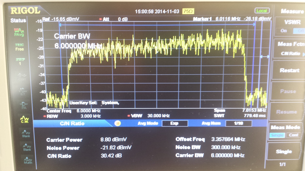
The tuner outputs a new Intermediate Frequency (I/F) at 6MHz, just like this second image. In this case we took a probe from a spectrum analyzer and measured the I/F out of the tuner to demonstrate the signal has moved from 579MHz to 6MHz.
Due to the fact TV Tuners sample and down-convert signals to I/F’s, and the I/F is passed from the tuner to the Digital Demodulator, the job of the demodulator is greatly simplified. I won’t discuss demodulators here, as I want to focus on "When things go wrong with tuners!".
 Look at this third image, its a measurement taken from a tuner project I recently worked on.
For the life of me I could not understand why my demodulator was not locking. I scratched my head
for a few minutes then tried to figure out whether I had a tuner programming issue, resulting
in a poor I/F being produced by the tuner (and given to the demodulator) or a demodulator
programming issue. The answer, ALWAYS, is to inspect the I/F coming from the tuner.
Look at this third image, its a measurement taken from a tuner project I recently worked on.
For the life of me I could not understand why my demodulator was not locking. I scratched my head
for a few minutes then tried to figure out whether I had a tuner programming issue, resulting
in a poor I/F being produced by the tuner (and given to the demodulator) or a demodulator
programming issue. The answer, ALWAYS, is to inspect the I/F coming from the tuner.
Images two and two should be generally identical, clearly something was wrong. Clearly the I/F coming from the tuner looked bad, it looked nothing like a digital television image. I isolated the problem to the tuner, not the demodulator and fixed the tuner programming issue within a few minutes. Had I not done that, I could have been banging away - trying various demodulator fixes, with no effect.
Lessions learned, if you’re have locking issues, check your tuner I/F output when you can. Its a time saver.
When you’re working with USB devices you often need to measure the overall power consumed. You need to measure Current (Amps) and Voltage (volts).
Sometimes you’re trying to add power management support to a driver, perhaps the device feels hot even when its not being used. If this bothers you enough to investigate then you’ll probably end up modifying the device driver to control the power dynamically. Neat! You’ll need to validate your work by measuring power before and after any changes you make.
Another use case: Perhaps you’re not dealing with a heat issue, but perhaps the device is unstable in certain modes of operation. For example, Analog TV mode vs Digital TV mode. You might want to look at power consumption to understand the differences.
The USB2.0 specification generally states that USB2.0 compatible devices should draw no more than 500ma of current. Perhaps your unstable or warm device is going over the recommended power budget? (Sidenote: Most PC Motherboards will happily provide more than 500ma of current).
You can measure power a number of ways but if you want something relatively cheap and mostly accurate, for the price of a couple of large coffees, I have something to recommend, the AboveTek USB Current/Power Meter.
Checkout the Amazon pictures to see exactly how you connect it. You’ll see it goes in-line inbetween the USB cable from your device to your computer. The LCD display toggles between Volts and Amps and has precision to two decimal places.
For fun, I measured the current and voltage of a device independatly to see how reliable the AboveTek measurements were. The good news is that the Voltage measurement is accurate all the way down to 10mv. Slight downside, the Current reports lower than ideal values by approximately 20ma.
To put this into perspective, a USB device may draw 460ma of current from your PC USB port, the AboveTek word report it’s drawing more like 480ma. Not a big difference but an annoyance.
Should you buy one of these when you already have a perfectly good Multi-Meter? Probably yes. It takes five seconds to plug the device in and start taking measurements. By contrast, it probably takes you a minute or so to grab the meter, connect the probes, find your magic inline usb power cable or special power break-out do-hickey widget.
When I’m working on non-company projects at 3am, it now only takes a moment to take a quick USB power measurement.
Based on measured usage, the AboveTek device consumes 20ma of current and automatically attempts to compensate for its own power burden in the resulting LCD information.
Copyright © 2025 Steven Toth